

TL;DR
Imec, ASML, and TSMC have integrated both n-type and p-type 2D transistors on a single wafer at a 50nm pitch, the tightest to date. This development signals significant progress toward scaling beyond traditional silicon limits, potentially marking a step toward post-silicon electronics.
Imec, ASML, and TSMC have demonstrated the integration of both n-type and p-type 2D transistors on a single 300mm wafer at a 50nm contact pitch, the most tightly packed to date for such devices. This achievement marks a critical step toward scaling beyond traditional silicon technology, with potential implications for the future of microelectronics.
The three organizations presented their work at the IEEE/JSAP Symposium, showcasing the ability to print channel lengths as short as 28nm using a single EUV exposure. The integrated transistors employ molybdenum disulfide (MoS2) for n-channel devices and tungsten diselenide (WSe2) or tungsten disulfide (WS2) for p-channel devices. According to reports, 94% of the transistors switched correctly, with an on/off current ratio exceeding 100,000, demonstrating high performance and reliability.
This integrated 2D transistor technology was achieved on a 300mm wafer, a significant milestone because it aligns with the scale used in current semiconductor manufacturing. The work indicates that atomically thin 2D materials could be scaled down to dimensions comparable to or even smaller than those of leading-edge silicon transistors, challenging existing limits of Moore’s Law.
Implications of 2D Transistor Integration for Future Chip Scaling
This development is significant because it demonstrates the feasibility of using atomically thin 2D materials to achieve transistor scaling beyond the limits of silicon. If scalable, this technology could enable smaller, faster, and more energy-efficient chips, potentially extending Moore’s Law or replacing silicon in future electronics. It also opens pathways for integration of diverse materials on a single wafer, advancing the design of complex, high-performance devices.
While the results are promising, the technology is still in early stages, and challenges remain in manufacturing consistency, large-scale integration, and commercial viability. Nonetheless, this marks a notable step toward a post-silicon era, where 2D materials could become a core component of next-generation microelectronics.

BOJACK 10 Values 250 Pcs A1015 BC327 BC337 C1815 S8050 S8550 2N2222 2N2907 2N3904 2N3906 PNP NPN Power General Purpose Transistors Assortment Kit
BOJACK High Quality Power Transistors Assortment Kit.
As an affiliate, we earn on qualifying purchases.
As an affiliate, we earn on qualifying purchases.
Progress Toward Post-Silicon Transistor Technologies
Current silicon transistor technology is approaching physical and economic scaling limits, with industry giants investing heavily in alternative materials and architectures. The demonstration by Imec, ASML, and TSMC builds on previous research into 2D materials like MoS2 and WSe2, which have shown promise for ultra-thin, high-performance transistors. The work aligns with broader industry efforts to find new pathways for continued device miniaturization amid the impending end of traditional silicon scaling, often referred to as the post-silicon era.
Prior to this, research has shown that 2D materials can be used to create transistors with excellent electrical properties at small scales, but integrating both n-type and p-type devices at such tight pitches on large wafers has been a challenge. This week’s demonstration represents a milestone in addressing those manufacturing hurdles and moving toward practical, scalable solutions.
“This is a significant step toward integrating 2D materials at scales compatible with current semiconductor manufacturing, potentially enabling a post-silicon future.”
— an anonymous researcher from Tom’s Hardware: For The Hardcore PC Enthusiast
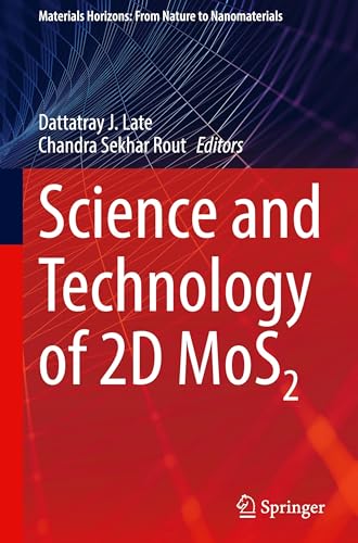
Science and Technology of 2D MoS2 (Materials Horizons: From Nature to Nanomaterials)
As an affiliate, we earn on qualifying purchases.
As an affiliate, we earn on qualifying purchases.
Unresolved Challenges for Commercial Deployment of 2D Transistors
It is not yet clear how scalable this technology will be for mass manufacturing, or whether issues such as uniformity, defect rates, and integration with existing processes can be effectively managed. The long-term reliability and cost-effectiveness of 2D transistors at commercial scale remain to be demonstrated, and further research is needed to address these hurdles.

Dual-Rail Wafer Cutter, Precision Silicon Wafer Scribing Machine with Diamond Blade, Adjustable Laboratory Semiconductor Glass Cutting Tool (Diamond Cutter Assembly)
Professional dual-rail wafer cutter designed exclusively for laboratory and semiconductor industry use, perfectly for cutting silicon wafer, glass…
As an affiliate, we earn on qualifying purchases.
As an affiliate, we earn on qualifying purchases.
Next Steps for Scaling and Industry Adoption
Researchers and manufacturers are expected to focus on refining fabrication techniques, improving yield, and testing the long-term stability of 2D transistors. Industry collaborations may also emerge to explore integration with existing silicon processes. The upcoming months will likely see further demonstrations and potential prototypes that could pave the way for commercial applications in high-performance computing and mobile devices.
ultra-fine transistor fabrication equipment
As an affiliate, we earn on qualifying purchases.
As an affiliate, we earn on qualifying purchases.
Key Questions
What are 2D transistors, and why are they important?
2D transistors use atomically thin materials like MoS2 or WSe2 to create ultra-thin, high-performance switching devices. They are important because they could enable continued scaling beyond silicon’s physical limits, leading to smaller, faster, and more efficient chips.
How does the 50nm pitch compare to current silicon transistor technology?
The 50nm contact pitch is comparable to the smallest features in advanced silicon chips, indicating that 2D transistors can be integrated at scales relevant to modern manufacturing processes.
What are the main challenges remaining before 2D transistors can be commercialized?
Major challenges include ensuring manufacturing consistency, reducing defect rates, integrating with existing fabrication infrastructure, and demonstrating long-term reliability and cost-effectiveness at scale.
Could 2D materials replace silicon in the future?
Potentially, if issues related to large-scale manufacturing and integration are resolved. Currently, 2D materials are viewed as promising candidates for extending or supplementing silicon technology.
Source: Tom’s Hardware: For The Hardcore PC Enthusiast