
TL;DR
ASML and Tata Electronics have signed an agreement to supply lithography equipment for India’s first commercial semiconductor fab in Dholera, Gujarat. The project, valued at $11 billion, aims to establish India as a key player in chip manufacturing. The deal was announced during Prime Minister Modi’s visit to the Netherlands.
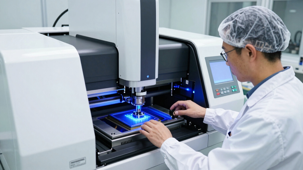
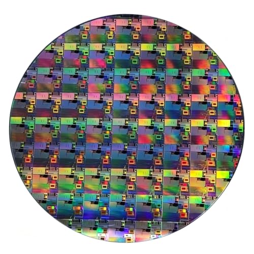
ASML has announced a partnership with Tata Electronics to supply lithography equipment for India’s first commercial semiconductor fabrication plant in Dholera, Gujarat. This marks a significant step in India’s efforts to develop a domestic chip manufacturing industry, with the project backed by a total investment of approximately $11 billion.
The deal was formalized during Prime Minister Narendra Modi’s visit to the Netherlands, where Dutch Prime Minister Rob Jetten was also present. The agreement covers the deployment of ASML’s advanced lithography tools, talent development initiatives, and supply chain support for the new 300mm fab. Civil construction at the Dholera site has reportedly reached about 50% completion, despite a major redesign late last year due to soil conditions. The redesign was necessary after soil testing revealed the ground was too soft and saline for the initial structural plans, but officials stated this would not delay the overall timeline. Trial production at the facility is still targeted for later this year, with full commercial operation expected to follow.
Why It Matters
This development is significant because it signals India’s serious push to enter the global semiconductor supply chain, reducing reliance on imports and fostering local industry. The partnership with ASML, a leading supplier of lithography equipment, indicates the country’s commitment to building cutting-edge manufacturing capabilities. The project’s success could reshape regional semiconductor dynamics and attract further investment in India’s tech ecosystem.
Silicon Wafer Lithography Sample, 6/8/12 Inch Single-Crystal Wafer for Semiconductor IC Circuit Demo, CPU Chip Display, CMOS Teaching & Exhibition (8" No.7F9+ + Stand)
Premium Single-Crystal Silicon High-quality silicon wafer designed for circuit demonstrations, lithography samples, and semiconductor education.
As an affiliate, we earn on qualifying purchases.
As an affiliate, we earn on qualifying purchases.
Background
India has long aimed to establish a domestic semiconductor manufacturing industry, but progress has been slow due to technological and infrastructural challenges. The recent announcement follows years of government initiatives and international partnerships to accelerate this goal. The Dholera project, announced in 2022, is part of India’s broader semiconductor vision, which includes attracting global players and developing local talent. Civil construction has been ongoing, with recent delays due to soil issues, but the project remains on track with trial production planned for later this year.
“This partnership marks a new chapter in India’s technological journey, bringing world-class semiconductor manufacturing to our shores.”
— Indian Prime Minister Narendra Modi
“Our collaboration with India on this project demonstrates the strength of international cooperation in advancing high-tech industries.”
— Dutch Prime Minister Rob Jetten
“Securing ASML’s lithography equipment is a critical step for India to develop a competitive, high-quality chip manufacturing ecosystem.”
— An industry analyst (unnamed)
300mm wafer fabrication tools
As an affiliate, we earn on qualifying purchases.
As an affiliate, we earn on qualifying purchases.
What Remains Unclear
Details about the specific timeline for full production, the scale of future expansion, and the involvement of other international partners remain unclear. It is also uncertain how quickly India will achieve self-sufficiency in semiconductor manufacturing and whether additional facilities will follow.

The World’s Most Important Machine: The Science Behind EUV Lithography
As an affiliate, we earn on qualifying purchases.
As an affiliate, we earn on qualifying purchases.
What’s Next
Next steps include completing civil construction, installing and testing ASML’s lithography equipment, and initiating trial production later this year. Monitoring the progress of these phases will be crucial in assessing the project’s success and timeline.

Setcas KW-4BC Spin Coater lab Coating Equipment for chip Manufacturing
Substrate size: 5-120mm(5 inches)
As an affiliate, we earn on qualifying purchases.
As an affiliate, we earn on qualifying purchases.
Key Questions
When is the Dholera fab expected to start production?
Trial production is targeted for later this year, with full commercial operation expected subsequently. Exact dates have not been publicly confirmed.
What role will ASML play in India’s semiconductor industry?
ASML will supply advanced lithography equipment, which is essential for high-volume chip manufacturing, enabling India to develop a technologically advanced fab.
Are other international companies involved in the Dholera project?
The current focus is on ASML and Tata Electronics, but additional partnerships or suppliers may be announced as the project progresses.
How does this project impact India’s global tech ambitions?
It positions India as a potential key player in the global semiconductor supply chain, reducing dependency on imports and attracting further high-tech investments.