
TL;DR
TSMC, Intel, and Samsung have announced their 2nm process technology roadmaps, each with distinct focuses and timelines. TSMC emphasizes predictable scaling, Intel pursues aggressive innovation, and Samsung prioritizes yield improvements. These developments impact the future of high-performance chips and global semiconductor supply.
TSMC, Intel, and Samsung have each announced their plans to advance into 2nm-class chip manufacturing, marking a significant milestone in semiconductor technology. These developments are crucial as they set the stage for future high-performance computing, AI, and mobile applications, impacting global supply chains and technological competitiveness.
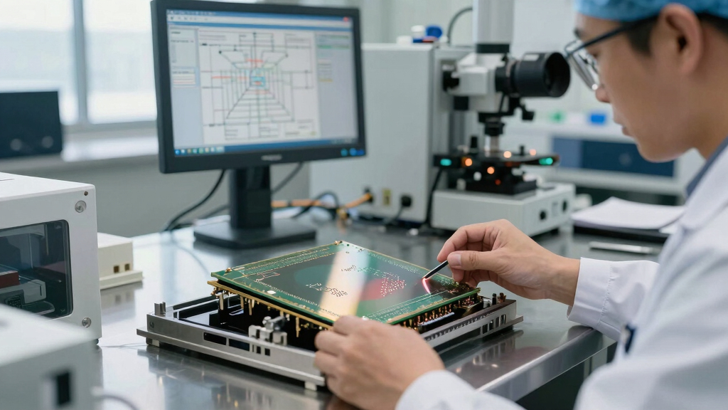
TSMC began high-volume manufacturing of its N2 process at two Taiwan fabs in December 2023, focusing on predictable scaling and specialization, with a split between high-performance and cost-effective nodes. Intel announced its 18A node, with mass production expected in late 2025, emphasizing the integration of GAA transistors and PowerVia backside power delivery, aiming for aggressive innovation with planned nodes up to 14A by 2028. Samsung, which started production with its SF2 node in mid-2025, is primarily focused on yield improvements and iterative development, with its GAA technology still facing yield challenges. While TSMC and Intel target high-performance applications, Samsung’s roadmap appears more cautious, prioritizing yield stability over scaling advancements.
Why It Matters
This trio’s roadmap announcements highlight differing strategies in the race for advanced semiconductor nodes. Intel’s aggressive push aims to regain technological leadership, potentially disrupting market dynamics. TSMC’s focus on predictable scaling sustains its dominance in high-performance chips, while Samsung’s emphasis on yield stability reflects its cautious approach amid manufacturing challenges. These strategies will influence supply availability, chip performance, and the competitive landscape for years to come.

Cooler Master Hyper 212 Black CPU Air Cooler – 120mm High Performance PWM Fan, 4 Copper Heat Pipes, Aluminum Top Cover, Low Noise & Easy Installation, AMD AM5/AM4 & Intel LGA 1851/1700/1200, Black
Cool for R7 | i7: Four heat pipes and a copper base ensure optimal cooling performance for AMD…
As an affiliate, we earn on qualifying purchases.
As an affiliate, we earn on qualifying purchases.
Background
Leading-edge process technology development has accelerated over recent years, with TSMC, Intel, and Samsung investing heavily to shrink transistor sizes and enhance performance. TSMC was the first to initiate 2nm high-volume production in late 2023, followed by Samsung’s mid-2025 start with its SF2 node, and Intel’s November 2023 launch of its 18A node, which is still in development lines. Historically, these companies have followed different paths: TSMC emphasizes specialization and predictable scaling, Samsung has prioritized technology iteration and yield, and Intel has pursued aggressive innovation with new transistor architectures and lithography techniques. The current landscape reflects a competitive push to lead in process technology, driven by applications in AI, mobile, and data centers.
“Our N2 process is designed to deliver predictable scaling and specialization, supporting a broad range of high-performance and cost-sensitive applications.”
— TSMC spokesperson
“Intel’s 18A node will incorporate GAA transistors and PowerVia to deliver industry-leading performance and power efficiency, with mass production targeted for late 2025.”
— Intel spokesperson
“Our focus remains on improving yields and stability at the 2nm node, ensuring reliable production before scaling further.”
— Samsung representative

ASRock Radeon AI PRO R9700 Creator 32GB Professional Graphics Card, 2920 MHz Boost Clock, GDDR6, AMD RDNA 4, AI-Accelerators, DisplayPort 2.1a, PCIe 5.0, Blower Cooler
Professional AI & Creator Workstation: AMD Radeon AI PRO R9700 GPU with 32GB GDDR6 is engineered for AI…
As an affiliate, we earn on qualifying purchases.
As an affiliate, we earn on qualifying purchases.
What Remains Unclear
While production timelines for TSMC and Intel are relatively clear, Samsung’s yield improvement efforts suggest potential delays or slower scaling. The exact adoption of High-NA EUV lithography and the pace of yield improvements remain uncertain, and whether Samsung can catch up in process maturity is still unresolved. Additionally, the impact of these technological advancements on market share and application-specific performance is yet to be determined.
Fundamentals of Semiconductor Manufacturing and Process Control (IEEE Press)
As an affiliate, we earn on qualifying purchases.
As an affiliate, we earn on qualifying purchases.
What’s Next
TSMC is expected to ramp up high-volume production of N2 chips through 2024 and 2025. Intel aims to begin mass production of 18A in late 2025, with subsequent nodes following through 2027–2028. Samsung will continue refining yields at its 2nm node, with broader adoption likely contingent on yield stability and process maturity. Industry analysts will closely monitor manufacturing yields, performance benchmarks, and customer adoption of these nodes.

Leofoto MPL and MPL-2 Multi-Function Tool, Handy Survival Multi-Tool, Photographers Allen Wrench Kit, Carabiner for Tripod (MPL)
Camera multitool and photography tools
As an affiliate, we earn on qualifying purchases.
As an affiliate, we earn on qualifying purchases.
Key Questions
When will TSMC start mass production of its 2nm chips?
TSMC began high-volume manufacturing of its N2 process in December 2023, with ongoing ramp-up expected through 2024 and into 2025.
What is Intel’s timeline for its 18A node?
Intel aims to begin mass production of its 18A node in late 2025, with subsequent nodes like 14A targeted for 2027–2028.
Why is Samsung’s approach different from TSMC and Intel?
Samsung is prioritizing yield improvements and process stability at its 2nm node, which has led to a more iterative development cycle compared to the aggressive scaling strategies of TSMC and Intel.
How might these developments affect the global chip market?
Advancements in 2nm technology could lead to more powerful, efficient chips for AI, mobile, and data center applications, potentially shifting market leadership and supply dynamics over the next few years.